
Latest Research Highlights
Enhanced Visible-Light Response and Optoelectronic Properties of a-IGZO Phototransistors with Dye and PMMA Blend Heterojunctions (ACS Appl. Electron. Mater. 2026, 8, 4, 1716–1725)
More about this work

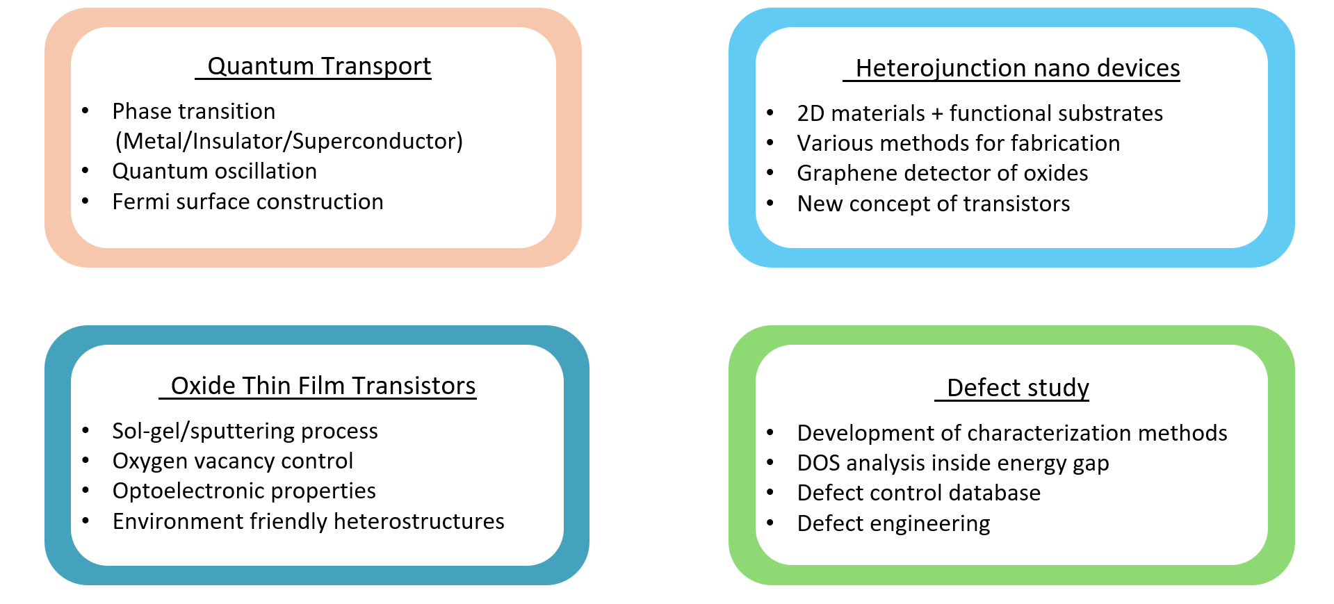
We study defect physics and device characterization to understand and quantify how defects impact material and device performance. We conduct quantum transport measurements under extreme conditions (e.g., low temperatures and high magnetic fields) to uncover fundamental transport mechanisms. We also develop heterojunction nanodevices by engineering interfaces and band alignment, and we advance oxide thin-film transistors by optimizing process–structure–property relationships for improved device operation.
Enhanced Visible-Light Response and Optoelectronic Properties of a-IGZO Phototransistors with Dye and PMMA Blend Heterojunctions (ACS Appl. Electron. Mater. 2026, 8, 4, 1716–1725)
More about this work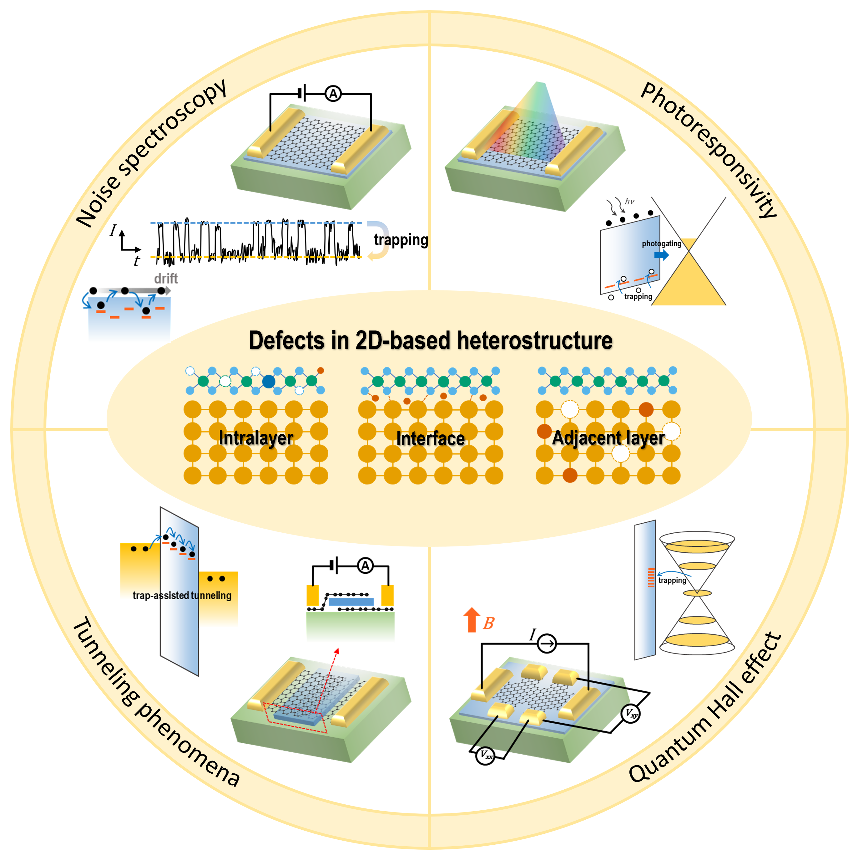
Review: Electrical probing of defects in two-dimensional material-based heterostructures
More about this work최신 소식이나 공지 내용을 이 카드에 넣으면 됩니다.